


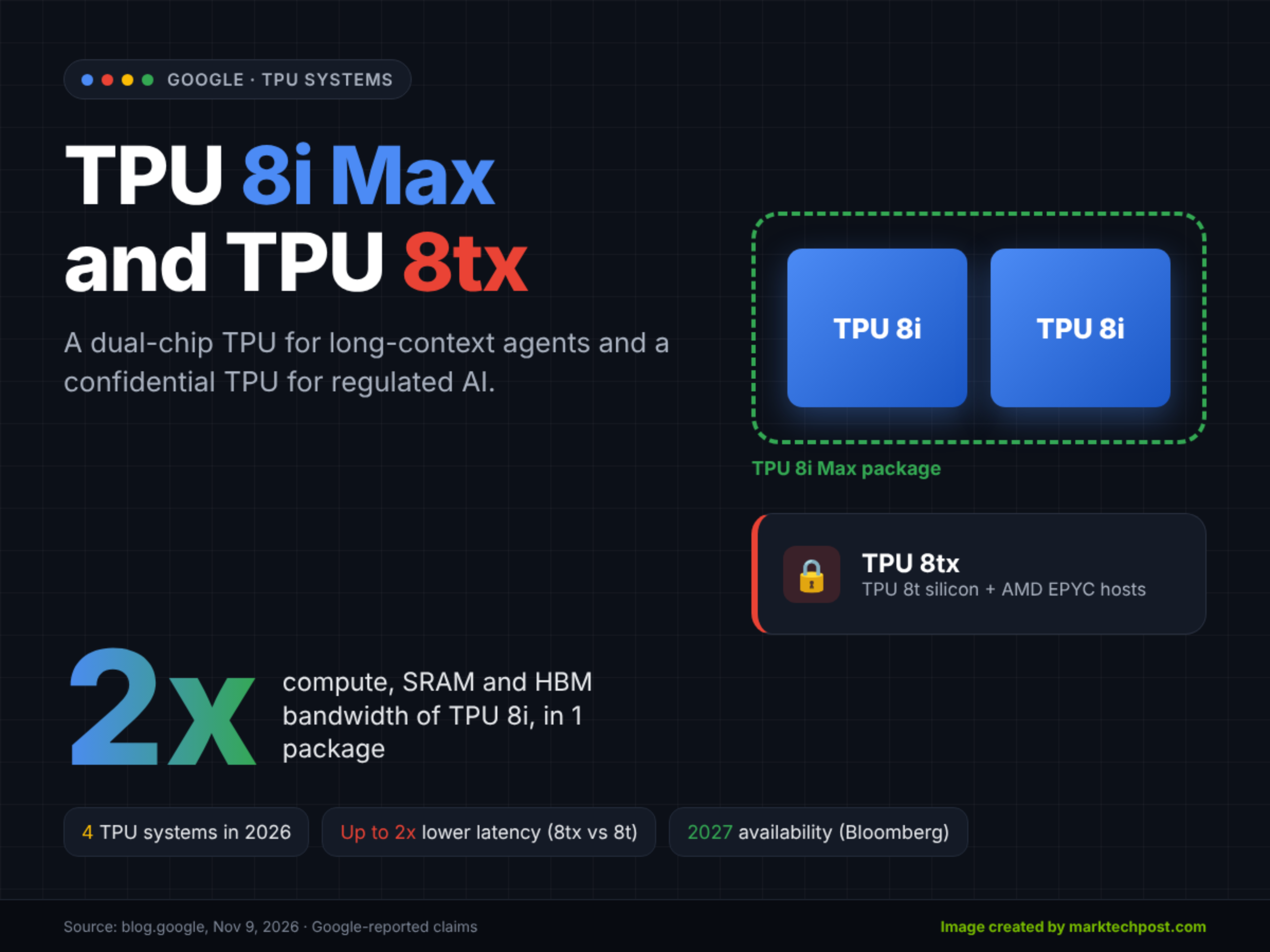
Google has added two new systems to its eighth-generation TPU lineup. TPU 8i Max targets massive context windows and rack density. TPU 8tx targets secure, confidential inference. Google TPU 8i Max is a dual-chip package built from 2 TPU 8i chips. Both arrive alongside TPU 8t and TPU 8i, announced in April.
Google announced both systems today. These are new system configurations, not new chips. Google reuses its existing eighth-generation silicon and changes packaging, hosts, memory and networking around it.
TPU 8i Max attacks the memory wall. Google team combines 2 low-latency TPU 8i chips onto 1 package. The result doubles compute, SRAM and HBM bandwidth compared with TPU 8i.
Each TPU 8i chip is rated at 10.1 PFLOPS of FP4, 288 GB of HBM and 8,601 GB/s. It also carries 384 MB of on-chip SRAM. Doubling those figures implies about 20.2 PFLOPS FP4, 768 MB SRAM and 17.2 TB/s per package. Google did not publish these absolute figures. It also did not state HBM capacity for TPU 8i Max.
Source: MarkTechPost — Read the full article on the original site ↗